Technology
Precision joining for photonic excellence
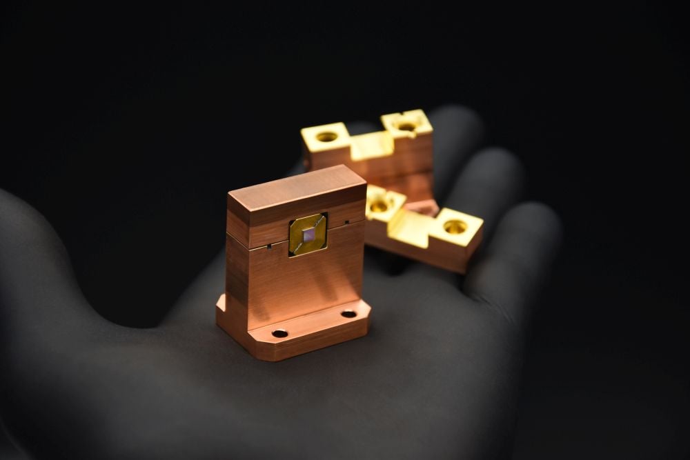
At PHOTONICPARTS, we specialize in high-performance packaging and assembly solutions for laser and photonic components. Our core expertise lies in flux-free-vacuum soldering, packaging technologies, robust thermal management, and hermetic sealing technologies. From laser crystal packaging to complex optics and subsystems for quantum, we integrate optical elements in a reliable and scalable manner thanks to our advanced joining processes. Whether it’s for highpower laser cooling, quantum applications, or aerospace-grade components – our solutions are made to last and withstand harsh environments.
Our Services
Soldering Technology
large area solder technology
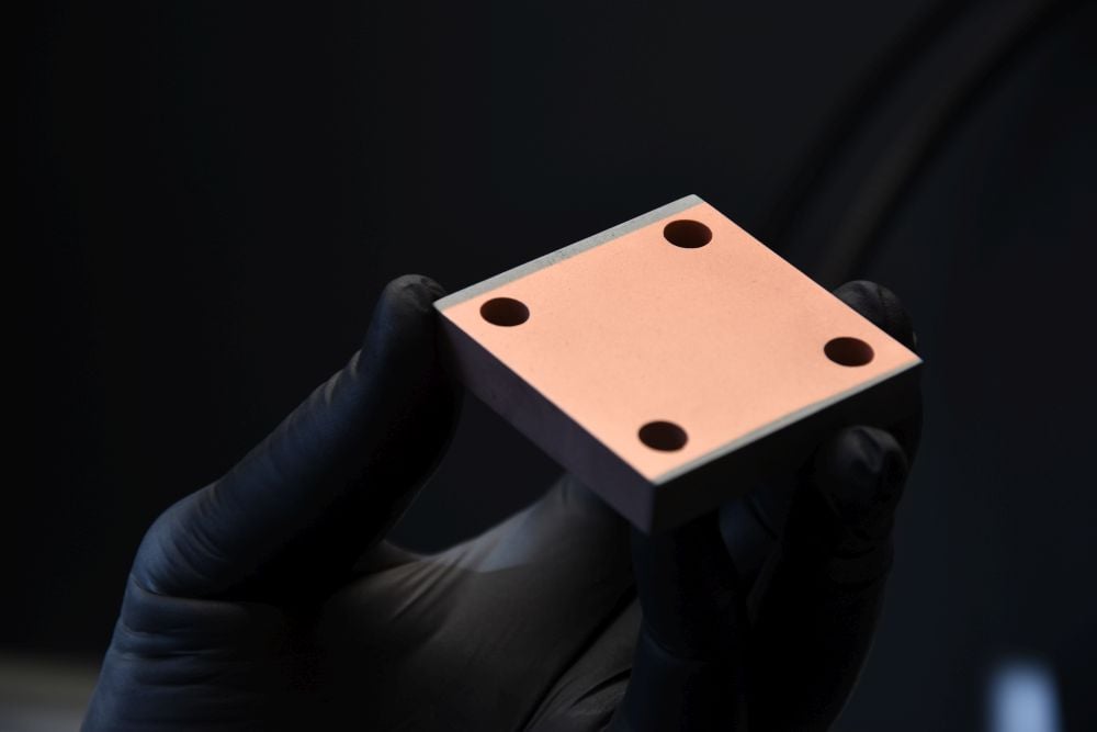
To establish a solder-based joint, a series of intricate activation steps are imperative to ensure the suitability and long-term stability of the materials involved. Central to this process are coating techniques applied through methods like PVD (Physical Vapor Deposition), magnetron sputtering, and galvanic processes. PHOTONICPARTS possesses both the expertise and the necessary equipment to carry out these processes, and we collaborate with external partners in the field of electroplating. Moreover, the precise application of thermal energy and comprehensive process control play key roles in soldering technology. PHOTONICPARTS boasts substantial expertise in vacuum soldering techniques and soldering without the use of flux support.

Layer Design
Customization of layer stacking to ensure longtime adhesion
Our technology empowers us to effectively join almost every solid materials. The ability to freely select materials offers significant advantages in tailoring the design of each specific joint. For instance, it enables us to adjust the thermal expansion coefficients of the joining materials to minimize material stresses, or to introduce thermal or electrical insulation through precise layering.
The unique structure of each joint is precisely crafted, taking into account the physical characteristics of the materials being joined and the intended purpose of the application.

Active Solder Alignement

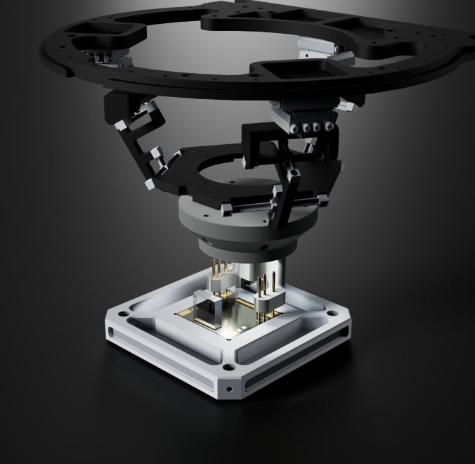
Optical components for machine-assisted assembly
- Repeatedly adjustable in liquid solder
- Fully integratable in machine-assisted automation setups
- Completely glue-free, UV/vacuum/space-compatibility
- Integrated heater and temperature sensor
